
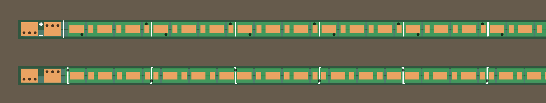
ThinkPad Daylight LED Strip #1 and #2
for the X60, X60s, X60t, X61t, X61s, and X61t in particular

 gEDA PCB source (v1)
gEDA PCB source (v2)
gEDA PCB source (v1)
gEDA PCB source (v2)
 Gerber files (v1)
Gerber files (v2)
Gerber files (v1)
Gerber files (v2)
 BOM
BOM
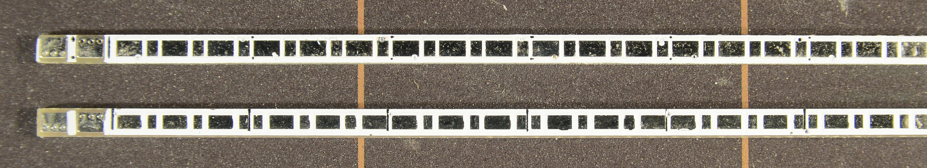
LED strips v1 and v2 are custom layouts designed specifically for the Nicha 157 package. Both versions place the LEDs so close as to be only a few thousandths of an inch from touching; in practice, many of the LEDs do in fact touch after reflow.
The specific NSSW157F-HG LEDs in use have exposed electrical test points on all four sides; this proved to be a significant liability when making v1 strips, as any solder that got between the LEDs during reflow could cause a short between groups of threes. The v2 strips reverse every other group such that any adjacent test points share the same electrical node.
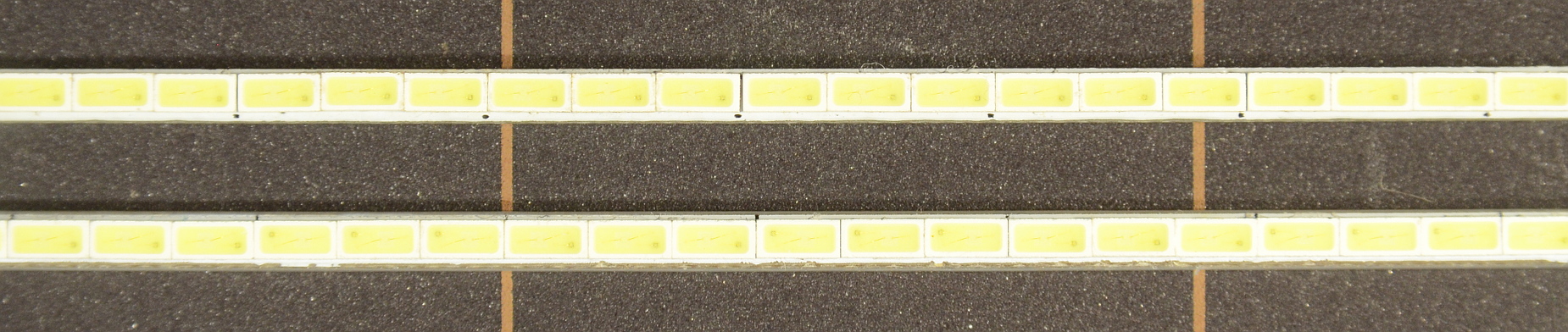
When viewed before installation, the light output of a v2 strip appears to have an almost pseudo-random pattern with slighty dimmer and slightly brighter spots; this is an illusion caused by the reversed groups. Interestingly, the altered light pattern also appears to help break up and further mitigate any remaining rippling and shadowing on SXGA screens.
v2 strips also very slightly reduce the spacing between LEDs, resulting in a lit-area that is about 2mm shorter on a 4:3 12.1" screen. This eliminates the 'bright corners' often seen on SXGA screens when an LED is too close to the left or right waveguide edge.
Note that on v1 strips, the outer solder point is LED- and the inner point is LED+. This is reversed on v2 strips in order to better accomodate CCFL-style solder tails with thicker insulation on the LED+ lead.